Welcome to my blog!


From the beginning of February it took 12 Friday afternoon labs to design and build this project, which is basically a computer controlled tactile object recognition system, called a Matrix Sensor. This device communicates with the computer using the parallel port and enables the outline and weight of an object to be displayed on a screen using a Graphic User Interface that was created with the latest version of Microsoft Visual Studio. There are a few parts to the hardware. The Switchboard, which consists of a 4x4 (16) mechanical array of on/off switches, a Force Sensing Resistor (FSR), which provides a force measurement system that, is interfaced to a range of electronic circuits. An ADC single sided board and a multiplexer double sided board. 

In the first part of this project, the schematics for the ADC and the Multiplexer boards were handed out on A4 prints. From these they were then created using Cadstar 12 and transferred to PCB artwork design. Once printed onto transfer paper, the designs could then be used to transfer the design onto PCB boards by using UV lights. The boards were then placed in a chemical for Developing and using another chemical for Etching away the copper, leaving the tracks exposed. The next step was to protect the copper tracks by a process called thinning which leaves a protected coat of tin alloy over the tracks. With the two boards finished in the chemical room, the artwork for the switchboard was then handed out on transfer paper to be completed with the same method.

A kit containing the required components for the three boards was handed out and each pad on the boards was dot punched before drilling could begin. Each pad for the components was drilled using a 0.8mm drill bit and a 1mm drill bit was used for the pin connecter pads. The drilling had to be precise to enable connectivity when soldering to the pads. The next part was to begin soldering the components onto the boards and are inter-connected with a 14 pin connector cable that brings the digital signals from the ADC board to the Multiplexer board and an 18 pin connector cable which brings 16 digital signals from the switchboard to the Multiplexer board. (The remaining two pins are for Gnd and power to the switchboard). Once this was completed, a visual check was carried out to examine the solder joints. A Continuity test was then done to check the signals between the IC’s along with its Gnd and power connections and was recorded on an Excel spread sheet. Also recorded were a Power pin test and a Functional test.

The final stage of the project is to interface the hardware with the Software. A basic working version of the software was provided that needed to obtain the correct addresses of the Parallel port on the PC to transfer the signals.  The Data port is 8 bits (0-7) and is from pin 2 to pin 9.This reads the values from the ADC.  The data port address is 888 Dec and each data line has its own Gnd line to eliminate noise. The Status port has 8 bits (0-7) but are inputs only which reads in data from the MUX and it’s address is 889 Dec. Pin 7 is hardware inverted which means if it reads a logic 1 it is reading 0V, and if it reads a logic 0 then it is 5V.  The Control port has another 8 bits (0-7) and allows another 4 pins for use as inputs or outputs. Pins 1, 14 and 17 are hardware inverted. Pin 14 acts as the MUX reset and pin 17 for the clock signal. The address of the Control port is 890 Dec.

Note:

ADC conversion is a process by which an analog quantity is converted to digital form.

Multiplexer is a device that takes in digital data from several sources and prepares it to one single source for the destination.

Progress Report


Week 12
It is the final lab now before the Easter break and the last chance to have everything working proparly. Today is the day for hand up of the hardware and software. Last week I was having problems with the way the switches were working along with the FSR. After some further testing on the switch board and with the logic, it proved to be one of the AND chips that was faulty. This was replaced and everything worked properly. In the next two weeks I will be working on the report for this project and there will be a powerpoint presentation to prepare for the end of semester.

Week 11
A few problems came to light this week. It came to my attention that I was only getting 3.8V into the board from a 5V output from the voltage source. After some testing it was discovered that the plastic washer on the positive jack lead was the cause. This was corrected by filing it down by .5 mm to allow a better grip at the back of the board and allowing a second nut so that a proper connection  could be made.
After this problem was fixed then it came to the software for the next one. The switches worked fine with the software but the FSR on th ADC board was giving problems, and as soon as I got that working the switches started to give trouble. As it stands I have a slight problem. When I press switch 1, that and switch 16 light up, and when I press 16, switch 15 lights up. I think it might be something to do with the AND chips more so than an error in the software. Next Lab is the last before the Easter break so I hope to have all these errors finnished with before the end of that Lab.

Week 10
 The software was built using Microsoft’s Visual basic 2010 version that was used to create the GUI for the hardware. When a switch is pressed on the switch board it will light up its corresponding switch on the screen. The ADC value on the GUI ranges from minimum 0 to maximum 255 and it’s the tactile sensor which reads an ADC value for the weight of the object and then this information could be converted to the correct weight of the object. 

 In order to obtain the correct addressing from the Parallel port to the software a formula was used.
For example:

Position
Formula
Data
0
     2^0
1
1
     2^1
2
2
     2^2
4
3
     2^3
8
4
     2^4
16
5
     2^5
32
6
     2^6
64
7
     2^7
128


Week 9
Bench testing completed, just in time too. Also managed to mount the hardware
onto a plastic platform. It looks the part now and it is working up to this point , next
is to get the software working for it to run through the parallel port on the PC.

  
Week 8
 This week was time consuming and it took most of the class time for the bench
 testing. Found a slight problem with the resistor pack and managed to fix it in time.

As you can see from my work bench it was a busy week.


Week 7
The hardware is complete at this stage, and is inter-connected using a 14 pin connector 
that brings the digital signals from the ADC board to the Multiplexer board so they can be out-putted 
to the PC via the D-type connector, and an 18 pin connector which brings 16 digital signals from the switchboard to the Multiplexer board. (The remaining 2 pins are for Gnd and Power to the switchboard).
The continuity testing is complete for the 3 boards.


Week 6
Switch board complete and started soldering  its components. Continuity testing on the ADC and the Multiplexer boards was done today and the data stored in an Excel spread sheet. 

Week 5
 Making good progress in the labs. At this stage i have finished soldering the ADC board and  the Multiplexer board. The switch board had to be re-made because of bad contact with the pads.

Week 4
In the lab this week, the boards have been drilled and i have recieved a kit containing all the components needed for the project.

Week 3
Once the 2 boards were finaly made and finnised in the etching tanks we were handed the
schematics for the switch boards. Oncthis was designed and transfered to PCB it was then to etched onto a double sided board.
Switch board schematic
The Switch board brings its power from the Multiplexer board and consists of 16 switches and resistors.


Week 2
At this stage the schematics are in there PCB form, and now awaiting a turn in the chemical
 room as there is only room for 2 people at a time in there.
Multiplexer top side PCB

ADC art work
Here we can see the artwork from the bottom side of the board.
With the components switched on it gives a clearer understanding
of the lay-out of the board.

Week 1
In this first class we were just briefed on the project and were givin the schematics to work with.
Using Cadstar 12, the schematics would then be designed and later transfered to PCB.
Multiplexer schematic
The Multiplexer consists of a 14 pin connector (going to the ADC board), an 18 pin connector
(going to the switchboard) and a D-type 15 pin parallel port connector,which will be connected to a PC.
It has two multiplexer IC's, one counter IC and two quad-2-input NAND IC's. 

ADC schematic 
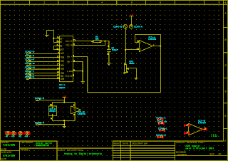
On the ADC board there is a 14 pin conector which is connected back to the multiplexer board.
An Analog to Digital converter (ADC0804), an Op Amp and an FSR connector.